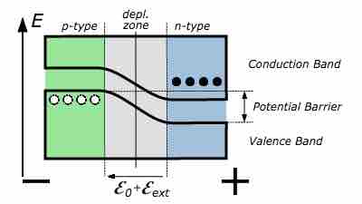
Reverse-biased p-n junction bands
Diagram of a p-n junction under reverse bias, showing conduction and valence bands, the depletion zone, the potential barrier, the resultant electric field,
Source
Boundless vets and curates high-quality, openly licensed content from around the Internet. This particular resource used the following sources: